


 Flexible Thinking: PCB Designers Still Wanted
 Connect the Dots: Five Best Practices for Designing Flex and Rigid-flex PCBs
 Tim’s Takeaways: Human Ingenuity and the Rigid-flex PCB
Insulectro and LCOA Install R&D Lab With Partner Kyocera in Orange County
March 7, 2023 | InsulectroEstimated reading time: 3 minutes
Insulectro, the largest distributor of materials for use in the manufacture of printed circuit boards and printed electronics, has opened a testing and development laboratory for Kyocera tools in its Lake Forest, California headquarters. The lab was created in association with backup and entry materials manufacturer LCOA in that company’s plant.
“I am pleased to announce that Insulectro, the exclusive North American distributor of drills, routers, endmills, and other cutting tools manufactured by Kyocera, will begin offering a variety of services from a new laboratory on our Lake Forest campus,” announced Geraldine Arseneau, Insulectro Product Manager for the Kyocera product line, “This will enable us to build on the synergy of Kyocera’s best-in-class tools and Insulectro’s dominance in drill room backup and entry products.” Arseneau joined Insulectro several years ago after a lengthy career with Kyocera.
The new lab is expected to support new product design, troubleshoot field issues, and include design feature testing, DoE (Design of Experiments) studies, confirmation testing, and repoint cycling testing.
It will determine proper feed and speed parameters for common PCB applications, develop processing parameters for new industry materials to understand how new technologies affect product performance, and supply customers with complete solutions. The Lab will also support industry and competitor benchmark studies.
Joe Negron, Kyocera Sales Manager, said, “The lab is a large next step for the Kyocera/Insulectro team. It vastly increases our capability to service our customers as technology changes.”
The Lab is equipped with a Schmoll drill/router (dual spindle drill with 160KRPM and router 50KRPM); a Microview CMM used to measure positional accuracy; and a Haas CM-1: compact CNC vertical machining center (50KRPM spindle, 5 HP motor).
It also includes a Struers automated polisher/grinder for X-sections; an Olympus Toolmakers microscope; and a metallograph to measure hole wall quality.
Insulectro Vice President of Product Management Michelle Walsh is also enthused about the additional capabilities, “This month we hosted a joint meeting of the Kyocera Team with Insulectro’s leadership and operations teams. We were all very excited not only about the Lab’s value for our existing customers but how we now have the capability to run studies to promote product offerings and qualifications requested by new customers. Fabricators can continue to count on Insulectro for the developing technological information.”
Kyocera SGS designs and manufactures tight tolerance precision carbide cutting tools for PCB applications. Products include drills, routers, end mills, and specialized cutting tools ranging from 0.05mm to 6.70mm diameters (0.0020" - 0.2638").
Kyocera’s renowned array of drills, routers, endmills, and specialty tools offer many benefits and advantages to customers for all their drilling and routing needs. Kyocera’s tool reliability and design flexibility are key strengths of their products, along with a complete R&D facility in the US, new tool manufacturing capability, and local technical resources, all available to support customer needs.
Insulectro supplies advanced engineered materials manufactured by Isola, DuPont, LCOA, CAC, Inc., Pacothane, Focus Tech, JX Nippon, TADCO, EMD Electronics (Ormet), Shikoku, Denkai America, ETI, Industrial Brush Corporation, Kyocera SGS Precision Tools, InduBond, and Shur-loc. These products are used by its customers to fabricate complex, multilayer circuit boards and to manufacture printed electronics components. Insulectro serves a broad customer base manufacturing rigid, rigid/flex, and flexible circuit boards for applications in a variety of end markets including aeronautics, telecom, data communications, high speed computing, mobile devices, military, and medical. Insulectro combines its premier product offering with local inventory across North America, fabrication capabilities and backed up by expert customer and technical support services.
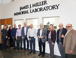
From Left to Right - Steve Komin, Senior Materials & Logistics Manager – Kyocera; Russ Reynoso, Design Engineering Manager – Kyocera; Geraldine Arseneau, Drill Product Manager – Insulectro; Curtis Vozar, Director of Material & Planning – Kyocera; Jeff Zaucha, Chief Financial Officer – Kyocera; Patrick Redfern, President & CEO – Insulectro; Dave Reiter, VP of Manufacturing – Kyocera; Tom Haag, President – Kyocera; Michelle Walsh, VP of Product Management – Insulectro; Joe Negron, Sales Manager PCB and MIT – Kyocera; Ken Parent, Chief Operating Officer – Insulectro.
Share on:


Suggested Items
Real Time with… IPC APEX EXPO 2024: Ventec Discusses New Pro-bond Family of Advanced Products
05/01/2024 | Real Time with...IPC APEX EXPOChris Hanson, Ventec's Global Head of IMS Technology, outlines the launch of four pro-bond formulas that deliver an outstanding combination of low dissipation factor (Df) with a dielectric constant (Dk) range to maximize the design window for critical PCB parameters. As Chris points out, Pro-bond is designed for low-loss, high-speed applications, while thermal-bond dissipates heat from a component through the board to a heat sink.
IPC's Vision for Empowering PCB Design Engineers
04/30/2024 | Robert Erickson, IPCAs architects of innovation, printed circuit board designers are tasked with translating increasingly complex concepts into tangible designs that power our modern world. IPC provides the necessary community, standards framework, and education to prepare these pioneers as they explore the boundaries of what’s possible, equipping engineers with the knowledge, skills, and resources required to thrive in an increasingly dynamic field.
iNEMI Packaging Tech Topic Series: Role of EDA in Advanced Semiconductor Packaging
04/26/2024 | iNEMIAdvanced semiconductor packaging with heterogenous integration has made on-package integration of multiple chips a crucial part of finding alternatives to transistor scaling. Historically, EDA tools for front-end and back-end design have evolved separately; however, design complexity and the increased number of die-to-die or die-to-substrate interconnections has led to the need for EDA tools that can support integration of overall design planning, implementation, and system analysis in a single cockpit.
Cadence, TSMC Collaborate on Wide-Ranging Innovations to Transform System and Semiconductor Design
04/25/2024 | Cadence Design SystemsCadence Design Systems, Inc. and TSMC have extended their longstanding collaboration by announcing a broad range of innovative technology advancements to accelerate design, including developments ranging from 3D-IC and advanced process nodes to design IP and photonics.
Ansys, TSMC Enable a Multiphysics Platform for Optics and Photonics, Addressing Needs of AI, HPC Silicon Systems
04/25/2024 | PRNewswireAnsys announced a collaboration with TSMC on multiphysics software for TSMC's Compact Universal Photonic Engines (COUPE). COUPE is a cutting-edge Silicon Photonics (SiPh) integration system and Co-Packaged Optics platform that mitigates coupling loss while significantly accelerating chip-to-chip and machine-to-machine communication.