


 The Chemical Connection: Reducing Etch System Water Usage, Part 2
 It’s Only Common Sense: Nice Guys Really Can Finish First
 The Right Approach: I Hear the Train A Comin'
Advanced Semiconductor Packaging Technologies: The Development Trend and the Growth Drivers, IDTechEx Reports
May 15, 2023 | PRNewswireEstimated reading time: 3 minutes
Advanced semiconductor packaging technologies are crucial due to the slowing of Moore's law and rising costs of monolithic Si IC development and manufacturing. Initially, components were individually packaged and integrated at the PCB board level, but as devices become smaller and require higher processing capabilities, component integration needs to be pushed beyond board level. Package level integration was the first advancement, followed by wafer level integration, which provides at least ten times higher connection density, a smaller footprint suitable for size-sensitive applications, and superior performance.
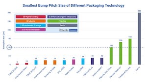
Wafer level integration encompasses fan-in, core fan-out, high-density fan-out, 2.5D IC, and 3D IC packaging technologies. However, only those with a bumping pitch size of less than 100 µm are considered as "advanced" semiconductor packaging technologies. This includes high-density fan-out, 2.5D IC, and 3D IC packaging technologies.
The shift from 2.5D hybrid integration to complete 3D vertical integration is crucial for future data-centric applications, and in this article, we will focus on this transition.
The primary challenge in the shift from 2.5D to 3D is to scale the size of the bumping pitch. In a 2.5D IC package, the bump pitch size ranges between 25 µm and 40 µm, depending on the interposer material. However, for a 3D stacking package, the bump size must be scaled down to a single digit µm or even lower down to below 1 µm dimension. TSMC has reported that the bump pitch for stacking N7/N6 chips is 9 µm and 6 µm for N5 chips stacking. This is expected to further decrease to 4.5 µm for N3 chip stacking and continue to decline for future generations of ICs. Stacking two chips with a small bump pitch size poses a significant challenge, as high-precision alignment on bonding dielectric materials must be achieved, especially at low temperatures. Additionally, proper control of Cu filling materials is necessary to prevent overflow during the bonding process. Furthermore, thermal management becomes a critical issue for packages with small bumping scales, which necessitates the consideration of package designs that enable better heat transmission and possible liquid cooling technologies.
The Growth Drivers
IDTechEx has identified four main application areas for advanced semiconductor packaging: high-performance computing (HPC) applications/data centers, communication networks, autonomous cars, and consumer electronics. The increasing demand for data processing is the primary driving force behind the growth in these application areas. However, each application has specific requirements that necessitate different advanced semiconductor packaging technologies.
For HPC applications/data centers, the priority is to provide superior data processing capabilities, making 2.5DIC technologies that use Si interposer or Si bridge the preferred option, despite their higher cost. In contrast, consumer electronics such as smartphones or smartwatches focus on miniaturization and cost, with organic-based packaging technologies being the top choice.
In 5G and beyond communication, the key challenge is transmission loss. Hence, advanced packaging technologies are used to bring the antenna closer to the RF IC chip, minimizing transmission loss. "Antenna-in-package (AiP)" is currently the most viable option for 5G mmWave, while "Antenna on chip/wafer (AoP)" is still under intense development to reduce costs.
For future autonomous vehicles, heterogeneous integration of CPUs and other components, such as HBM and reliable power delivery systems, will create new opportunities for advanced semiconductor packaging and innovation.
The expansion of data processing is the unifying growth factor for all these applications. However, as the requirements for each application area differ, advanced semiconductor packaging technologies are being used to meet specific needs.
IDTechEx has released a new market research study titled "Advanced Semiconductor Packaging 2023-2033". This study examines the market prospects, key player analysis, and most recent developments in advanced semiconductor packaging technologies. This report also conducts a comprehensive examination of the semiconductor market as a whole. Additionally, IDTechEx leverages its expertise and years of research in data centers, autonomous vehicles, 5G, and consumer electronics to provide the reader with a thorough understanding of how advanced semiconductor packaging is influencing various industries and what the future may hold.
Share on:


Suggested Items
Gartner Survey Finds 61% of Organizations Are Evolving Their D&A Operating Model Because of AI Technologies
05/01/2024 | Gartner, Inc.Sixty-one percent of organizations are forced to evolve or rethink their data and analytics (D&A) operating model because of the impact of disruptive artificial intelligence (AI) technologies, according to a new Gartner, Inc. survey.
Real Time with… IPC APEX EXPO 2024: Operational Excellence and Smart Factory Initiatives
04/30/2024 | Real Time with...IPC APEX EXPOOperational excellence and operational efficiency are defined in this interview with Koh Young General Manager Joel Scutchfield. He touches on automation, AI, and collaboration as solutions to resource limitations. Koh Young's data-driven approach uses AI for process adjustments, data analytics, and supply chain enhancements. The discussion underscores the shift toward smart factory initiatives and the future of manufacturing, with a focus on reshoring, nearshoring, and technology utilization.
IDTechEx Report on Quantum Technology: Nano-scale Physics for Massive Market Impact
04/30/2024 | PRNewswireThe quantum technology market leverages nano-scale physics to create revolutionary new devices for computing, sensing, and communications. Across the industry, quantum technology offers a paradigm shift in performance compared with incumbent solutions.
NASA’s Optical Comms Demo Transmits Data Over 140 Million Miles
04/30/2024 | NASA JPLNASA’s Deep Space Optical Communications experiment also interfaced with the Psyche spacecraft’s communication system for the first time, transmitting engineering data to Earth.
Real Time with… IPC APEX EXPO 2024: Insight into Summit Interconnect's Success
04/30/2024 | Real Time with...IPC APEX EXPOShane Whiteside, CEO of Summit Interconnect, discusses the company's recent recognition as one of the best PCB fabricators in the industry by receiving IPC's Peter Sarmanian award. Whiteside touches on the impact of changes in the marketplace, such as the Defense Production Act and presidential determination, on their growth. Whiteside also shares the company's focus on mechanical and data automation to enhance manufacturing processes and anticipates more automation and evolution in the industry.