


 Global Sourcing Spotlight: Golf, Friedman, and the Benefits of Global Sourcing
 Nolan’s Notes: Coming to Terms With AI
 The Knowledge Base: A CM’s Perspective on Box Build Practices
Process Control for Solder Paste Deposition
September 14, 1999 | SMTAEstimated reading time: 10 minutes
The authors, Mark Owen and Jeff Hawthorne, review solder paste inspection, the sensor technologies used to acquire 2-D/3-D inspection and measurement data, methods of using measurement data to identify problems and solutions, and guidance on developing an AOI strategy.
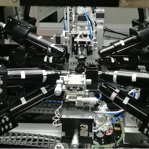
The use of automated optical inspection (AOI) in the SMT industry has grown dramatically. This growth has been driven by several factors, including improved AOI technology and decreased product and package sizes that have limited the effectiveness of manual inspection and in-circuit test (ICT). The most common process control points for SMT assemblies are after solder paste deposition, after component placement and post-reflow. Earlier work highlights the considerations in developing an overall process control strategy.1 This article focuses on AOI for solder paste deposition (Figure 1).
Why Inspect Solder Paste?
Several considerations make solder paste deposition a logical choice for inspection:
- A majority of solder joint defects have been traced to solder deposition defects.2
- Repair is much less expensive after paste deposition than after component placement, at least 10 times less expensive than after reflow, and at least 50 times less than after ICT.2
- Research has shown that for array packages, the measurement of solder paste volume is essential for controlling post-reflow yield.3,4,5
- Surface mount shields increasingly used on wireless communication products require effective paste deposition control because of the difficulty of repair or inspection after placement.
Equipment suppliers and electronics manufacturers have long recognized the need for increased monitoring and control of the paste deposition process. Printing equipment suppliers have provided sophisticated systems for measuring and controlling process parameters such as squeegee pressure, squeegee speed, snap-off height, etc. Automated screen printers use machine vision for the alignment of the stencil to the printed circuit board (PCB), and some systems offer optional AOI systems for post-process verification. In addition, many manufacturing operations have implemented storage, cleaning, and management procedures for paste and stencils, and have conducted numerous experiments to characterize the screen printing process.
The paste process has improved with these tools and procedures, but engineers have learned that there are just too many variables and random causes to only inspect the process. The product must also be inspected. In addition, the increasing demands of the SMT line (namely, higher density circuits, area-array devices, finer pitch components and surface mount shields) all provide strong justification for in-line inspection.
Measuring Defects
The addition of measurements of paste area, height, placement and volume can be used to more directly link visible defects with specific actions, as shown in Table 1.
Paste measurements also provide objective assessments of process and machine capability, which are useful when comparing systems or verifying them after line modifications.
Solder Paste Inspection Technology
Solder paste inspection systems use a variety of sensor technologies to obtain data on paste deposits:
- 2-D digital video. Video cameras can be used to perform fast and inexpensive inspection and measurement of 2-D characteristics such as paste area and position.
- 3-D laser triangulation. A structured lighting system and sensor can be used to determine 3-D paste characteristics such as height and volume. These systems often use a laser as the light source, and vary considerably in speed and accuracy.
- Hybrid systems. These systems take advantage of the speed and simplicity of 2-D video for measuring 2-D paste characteristics, and use a 3-D sensor to collect height and volume information at selected sites to ensure product quality and provide data for process control.
Laser triangulation is generally used for 3-D measurements. Laser systems have to correct for several technical issues: the color and transparency of the board materials; the specular reflections and shadows that cause a partial loss of data; a zero reference plane (usually the top of a trace or pad) to correct for warp; and axes alignment with scanning direction.
Several equipment suppliers have developed systems for the inspection and measurement of solder paste, and several manufacturers make in-line or off-line systems that use a single wavelength triangulation sensor. Some add additional detectors8 or use wider lines9 to correct for shadowing or specular reflections. A key consideration for the 3-D sensor is the data acquisition speed, which can severely limit the number of deposits on a board that can be measured in-line at production rates. One of the more sophisticated systems uses acousto-optic laser deflectors to speed up the collection of data.10 Another system scans with the triangulation sensor rotated 45°, which increases the data acquisition rate, minimizes the effects of shadows and specular reflections, and eliminates alignment- and axes-dependent effects (Figure 2).11
How Important Are 3-D Measurements?
Published work comparing the capabilities and requirements of AOI systems and the correlation between measurements and performance are few. XeTel researchers4 compare a 3-D laser triangulation system with 2-D/3-D vision system, and conclude that vision is preferred for most SMT paste deposits but laser systems are more accurate for very fine-pitch (less than 0.5 mm) devices. They also conclude that laser-based systems require a zero height reference position to give accurate results, and that vision systems are more accurate for fiducial alignment, correctly locating paste deposits and separating data between deposits. Burr2 concludes that solder paste volume is the single best predictor for finished board quality involving ball grid array (BGA) and chip scale package (CSP) devices. He also concludes that benchtop measurement tools do not eliminate reproducibility errors - i.e., variability between operators. Celestica/JPL consortia researchers6 note that in-line measurements are required for accuracy, but that laser 3-D measurements without properly designed surface reference pads were inaccurate. Therefore, they decided to check the in-line system with an off-line manual laser profiling system for verification.
Calculating the zero height reference (usually the height of pads and traces) is extremely important for achieving good accuracy and repeatability of 3-D measurements. Laser wavelength affects this calculation. Systems that use acousto-optic deflectors employ 830 nm (or near infrared) laser lines because of restrictions imposed by the deflectors` optical properties. While this technology can achieve much higher scan rates, the lasers penetrate into PCB materials. Accurate paste measurements therefore require that a zero height reference be measured on traces near each pad location. However, manually specifying these reference locations can takes days of programming per board. In some applications, such as CSP and BGA devices, local copper references are not available.
Other laser systems use 670 nm lasers that reflect off the soldermask so a local copper reference is not required during each inspection. This significantly simplifies programming because the Gerber data automatically programs the paste deposit locations. Information on trace locations is not required. Because these systems are measuring with respect to the solder mask, a correction must be made for the solder mask thickness. Some systems use a fixed offset for the paste thickness that will cause all mask variations to be included in the paste measurement.6 One technique11 uses a board without paste to calculate the nominal solder mask offset, then takes a measurement near the alignment fiducial to correct for board-to-board solder mask thickness variations (Figure 3).
Recent research has shown the critical relationship between solder joint volume and joint fatigue failure.3 This work shows that the number of cycles to failure is proportional to V~2, where V is the volume in cubic mils. Because the volume of the solder joint can vary by a factor of 10 from the smallest CSP and fine-pitch device to larger SMT components, it is essential to measure the volume accurately for the smallest paste deposits. Measurement precision to process tolerance ratios of 7 to 12 percent for various small-volume devices has been demonstrated using a hybrid technology machine similar to the one shown in Figure 2d.
To control joint failures, 100 percent 2-D inspection of all pads is essential. Furthermore, 3-D measurements are required for process control, particularly when CSP and other small-volume solder joints are used.
Developing a Solder Paste AOI Strategy
A large number of criteria can be used to evaluate solder paste inspection and measurement equipment for a specific application. The following considerations are important to the successful implementation of a solder deposition control system that meets the application objectives:
- Does the system identify random defects that can only be observed in the product?
- Does the system provide measurement data on significant parameters that can be used to ensure that the process is in control?
- Is the system cost-effective for the intended application?
- Is ease-of-use, including programming time, cycle time, and data formatting and analysis, adequate for the demands of the application and the user level?
The following examples compiled from OEM and contract assemblers that have recently implemented AOI for solder paste illustrate how these objectives were translated into measurable goals, equipment requirements, expected benefits and equipment choices:
- A power supply manufacturer that specializes in low-volume, high-mix, medium-complexity boards wants to optimize the paste deposition process through a series of designed experiments, resulting in decreased process variability. The primary requirement of the AOI system is to achieve a specified measurement repeatability and accuracy. Ease-of-programming and speed will impact the time required for data acquisition, but are secondary considerations. In-line capability is not a requirement, so a benchtop 3-D laser based system is appropriate. The desired benefits are decreased height and volume variability as measured by the standard deviations of the measured values, and increased process capability as measured by Cp and Cpk.
- A high-mix contract manufacturer (CM) that already has implemented solder joint inspection wants to increase first-pass yield. The primary requirements of the AOI system are in-line operation, speed and inspection capability. This is a high-mix application, so programming time is important, but statistical process control (SPC) measurement will not be implemented, and a 2-D vision based system with 100 percent coverage is appropriate. The desired benefit is to eliminate 75 percent of the defects found in solder joint inspection that can be attributed to the solder paste process.
- A cellular phone manufacturer uses a significant amount of array components and surface mount shields, and therefore requires the use of process monitoring to detect shifts or trends in the printing process. The primary requirements of the AOI system are the same as in the previous example - in-line operation, speed and inspection capability - but with the added requirement of accurate and repeatable measurement data. Because this is a high-mix environment, programming time is important, so a 2-D vision based system with 3-D sampling is chosen. The desired benefit is increased first-pass yield as measured at end-of-line test, with a goal of eliminating 90 percent of the defects presently attributed to the solder paste process.
These examples illustrate the importance of considering line cycle times, product mix and component types when developing a solder paste AOI strategy.
Conclusion
The solder paste deposition process is one of the most important and difficult steps in SMT assembly. Because of the large number of process variables, random defects that are difficult to predict or control can occur. The increased use of BGA, CSP and other array packages, as well as increased board density, compound the situation. As a result, solder paste deposition AOI is becoming increasingly popular, including 100 percent inspection of every board on many high-volume manufacturing lines. Solder paste measurements can be used to monitor the process, identify problems, indicate specific corrective actions, and track process quality and capability over time. Equipment suppliers offer a range of products to address varying solder paste AOI requirements, and an effective AOI strategy requires the careful selection of equipment which uses the sensor technology that matches the speed, mix and component type of the application.
REFERENCES
1 Jeff Hawthorne, Mark Owen and Pierre Allain, "Automated Optical Inspection for SMT," EMS Magazine, Vol. 2, 1999.
2 Donald Burr, "Printing Guidelines for BGA and CSP Assemblies," SMI `98, p. 417-24.
3 Jean-Paul Clech, "Flip Chip/CSP Assembly Reliability and Solder-volume Effects," SMI `98, p. 315-23.
4 Julian Partridge and Rick Gunn, "Paste Printing and Characterization for Chip Scale Package Assemblies," SMI `98, p. 405-24.
5 I. Sterian, et al., "Compatibility of CSPs in SMT Assembly," SMI `98, p. 225-30.
6 Scott Buttars, "Stencil Printing Principles and Parameters," Future Circuits International, Issue 1, Vol. 2, 1997, p. 159-64.
7 Alan Hobby, "Printing," SMT, April 1999, p. 66-74.
8 US Patent 5,862,973, January 26, 1999 by Teradyne Inc.
9 US Patent 5,495,337, February 27, 1996 by MVP Inc.
10 US Patent 5,654,800, August 5, 1997 by GSI.
11 Patent S80748, MV Technology Ltd.
MARK OWEN and JEFF HAWTHORNE may be contacted at MV Technology Ltd., Unit 3, IDA Enterprise Centre, Pearse St., Dublin 2, Ireland; (503) 439-1606; E-mail: sales@mvt.ie.

Figure 1. Solder paste inspection provides process control for the most complex process on the SMT line, and is essential for BGA and CSP components.

Figure 2. Solder paste sensor technologies: a) basic 3-D laser triangulation using a slit laser or projector, perhaps with addition of multiple detectors or thicker lines to reduce specular reflections; b) basic machine vision with ring lighting; c) use of higher speed acousto-optic laser deflector; and d) a hybrid approach using 3-D multi-axis scanning and machine vision.

Figure 3. Some lasers penetrate PCB materials, forcing trace or pad use as local reference planes.
Share on:


