


 It’s Only Common Sense: OCCAM—the Time Is Now
 Marcy's Musings: The Growing Industry
 Dan’s Biz Bookshelf: Seeing the How
Copper Laminates Made From Transparent Polyimide Films Now Available
August 26, 2016 | DKN ResearchEstimated reading time: 3 minutes
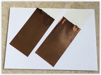
Significant progress has been made over the last few years in building transparent and heat resistant flexible circuits. Several transparent materials were developed along with special manufacturing processes. A copper laminate made from a thin transparent polyimide file plated with a copper layer on both sides for use in traditional manufacturing processes is now available. DKN Research developed a new copper metalizing process using transparent polyimide films. The new laminate will provide manufacturing capabilities using transparent flexible circuits for traditional printed circuit manufacturers.
Polyimide films are the primary substrate material for heat resistant flexible circuits because of the balanced performances between heat resistance and physical properties. The problem is they tend to have an orange or brown color, so the film’s transparency is very low. This is a huge barrier for any optical applications. PET films are another popular substrate material for transparent flexible circuits, but their heat resistance is too low and will not work in standard assembling processes such as soldering and wire bonding. A couple of new heat resistant resins such as LCP have been synthesized and are considered the next generation material for flexible circuits; however, they may not be transparent either. Many chemists used to question the availability of a product that is both transparent and heat resistant. That has changed. Several chemists were successful in synthesizing transparent polyimide resins, and a few companies have brought to market some thin transparent polyimide films that serve as the substrate for heat-resistant flexible circuits.
There are still a few technical hurdles in building transparent flexible circuits. The biggest one is the availability of an appropriate copper laminate for the standard photolithography/chemical etching process. Some of the copper laminates had problems with the surface treatment and gluing of the copper. The transparency of the circuits was remarkably reduced by absorption and scattering.
DKN Research developed a total solutions package for transparent flexible circuits based on each application. During the R&D process, DKN Research has established an electroless and electroplating process of nickel, copper and gold on the transparent polyimide films that provides thin copper laminates available for the standard photolithography/etching process of high density flexible circuits. The new copper laminate could be valuable for traditional flexible circuit manufacturers, because the new laminate does not need any additional equipment or chemicals to build transparent flexible circuits. The transparency of the circuits can be over 85%.
The standard construction of the laminate uses double-sided 3-micron thick copper layers on a 25-micron thick transparent polyimide film. The copper thickness can be thinner at 0.2 microns, and wider thickness ranges will be available for circuit manufacturers. The thin copper conductor could be valuable for semi-additive processes for ultra-fine flexible circuits with microvia holes in the transparent flexible circuits. DKN Research will provide free laminate samples along with a processing guide to circuit manufacturers.
DKN Research will upgrade the laminates and process capabilities to build the leading edge flexible circuits. DKN Research is happy to share the materials and information with circuit manufacturers and device manufacturers. Click here to view a short clip about their products and services.
About DKN Research
DKN Research is a global engineering leader for microelectronics and packaging, specializing in printable & flexible electronics. DKN Research has developed a broad range of leading edge technologies from materials to final devices based on customers’ requirements. They are capable of managing many kinds of materials and manufacturing processes to build and create new devices based on customer needs.
DKN Research provides a broad range of engineering and consulting services not only for the manufacturing community but also the R&D and quality assurance professionals. DKN Research welcomes all inquiries to assist in creating your own circuit devices using its broad range of processing technologies.
Share on:


Suggested Items
Designer’s Notebook: What Designers Need to Know About Manufacturing, Part 2
04/24/2024 | Vern Solberg -- Column: Designer's NotebookThe printed circuit board (PCB) is the primary base element for providing the interconnect platform for mounting and electrically joining electronic components. When assessing PCB design complexity, first consider the component area and board area ratio. If the surface area for the component interface is restricted, it may justify adopting multilayer or multilayer sequential buildup (SBU) PCB fabrication to enable a more efficient sub-surface circuit interconnect.
Insulectro’s 'Storekeepers' Extend Their Welcome to Technology Village at IPC APEX EXPO
04/03/2024 | InsulectroInsulectro, the largest distributor of materials for use in the manufacture of PCBs and printed electronics, welcomes attendees to its TECHNOLOGY VILLAGE during this year’s IPC APEX EXPO at the Anaheim Convention Center, April 9-11, 2024.
ENNOVI Introduces a New Flexible Circuit Production Process for Low Voltage Connectivity in EV Battery Cell Contacting Systems
04/03/2024 | PRNewswireENNOVI, a mobility electrification solutions partner, introduces a more advanced and sustainable way of producing flexible circuits for low voltage signals in electric vehicle (EV) battery cell contacting systems.
Heavy Copper PCBs: Bridging the Gap Between Design and Fabrication, Part 1
04/01/2024 | Yash Sutariya, Saturn Electronics ServicesThey call me Sparky. This is due to my talent for getting shocked by a variety of voltages and because I cannot seem to keep my hands out of power control cabinets. While I do not have the time to throw the knife switch to the off position, that doesn’t stop me from sticking screwdrivers into the fuse boxes. In all honesty, I’m lucky to be alive. Fortunately, I also have a talent for building high-voltage heavy copper circuit boards. Since this is where I spend most of my time, I can guide you through some potential design for manufacturability (DFM) hazards you may encounter with heavy copper design.
Trouble in Your Tank: Supporting IC Substrates and Advanced Packaging, Part 5
03/19/2024 | Michael Carano -- Column: Trouble in Your TankDirect metallization systems based on conductive graphite or carbon dispersion are quickly gaining acceptance worldwide. Indeed, the environmental and productivity gains one can achieve with these processes are outstanding. In today’s highly competitive and litigious environment, direct metallization reduces costs associated with compliance, waste treatment, and legal issues related to chemical exposure. What makes these processes leaders in the direct metallization space?