


 The Right Approach: I Hear the Train A Comin'
 It’s Only Common Sense: OCCAM—the Time Is Now
 Marcy's Musings: The Growing Industry
DARPA Researchers Develop Novel Method for Room-Temperature Atomic Layer Deposition
September 1, 2016 | DARPAEstimated reading time: 2 minutes
DARPA-supported researchers have developed a new approach for synthesizing ultrathin materials at room temperature—a breakthrough over industrial approaches that have demanded temperatures of 800 degrees Celsius or more. The advance opens a path to creating a host of previously unattainable thin-film microelectronics, whose production by conventional methods has been impossible because many components lose their critical functions when subjected to high temperatures.
Image caption: Pictured is a Gallium Nitride film deposited on a Silicon substrate at 27 degrees Celsius (80 degrees Fahrenheit) using an innovative process for depositing super thin films. Current deposition methods for these materials require temperatures around 800 degrees Celsius (1,472 degrees Fahrenheit), which is incompatible with microelectronics processing due to the damage that heat can wreak on underlying substrate materials.This new method could allow integration of previously incompatible microelectronics materials. (University of Colorado Boulder image)
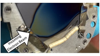
The new method, known as electron-enhanced atomic layer deposition (EE-ALD), was recently developed at the University of Colorado, Boulder (CU) as part of DARPA’s Local Control of Materials Synthesis (LoCo) program. The CU team demonstrated room-temperature deposition of silicon and gallium nitride—linchpin elements in many advanced microelectronics—as well as the ability to controllably etch specific materials, leading to precise spatial control in three dimensions. Such a capability is critical as the demand grows for ever-smaller device architectures.
After first demonstrating the process in early 2015, team members went on to perform detailed mechanistic studies to learn how best to exploit and control EE-ALD for film growth. By controlling the electron energy during the ALD cycles, they discovered that they could tune the process to favor either material deposition or removal. The ability to selectively remove (etch) deposited material with electrons under conditions as low as room temperature is unprecedented and is anticipated to enhance film quality. The group is also exploring other methods to etch specific materials—such as aluminum nitride and hafnium oxide, important in specialized electronics applications—showing that they can selectively etch these materials in composites, which provides an attractive alternative to traditional masking approaches.
CU has also built a custom deposition chamber to demonstrate industrial relevance and scalability of the EE-ALD process, which can deposit or etch films composed of multiple materials on industrial-scale six-inch silicon wafers. In principle, the method could be scaled to larger substrates and parallelized to process many wafers at once. The researchers are now working to understand the vast parameter space of the EE-ALD process to better control film composition and properties in three dimensions.
“Looking forward, the EE-ALD approach could serve not just as a tool for integrating incompatible materials but also more generally to build and etch device architectures at atomic scales, an increasingly important capability as circuit geometries shrink,” said Tyler McQuade, DARPA program manager.
CU’s work, which was performed in collaboration with the Naval Research Laboratory and National Institute of Standards and Technology, was recently recognized as one of six “Highlights of 2016”—selected from more than 400 accepted oral presentations and posters at the 16th International Conference on Atomic Layer Deposition in Dublin, Ireland.
Share on:


Suggested Items
Real Time with... IPC APEX EXPO 2024: Sustainability in the Industry
04/26/2024 | Real Time with...IPC APEX EXPOGuest Editor Henry Crandall and Chris Nash of Indium Corporation discuss the company's 90th anniversary and its focus on sustainability. They focus on the benefits of sustainable materials, their compatibility, and value propositions. The conversation also highlights how Durafuse LT technology's role in reducing reflow temperatures is leading to significant cost and energy savings. Nash also touches on downstream sustainability efforts such as using recycled materials for packaging.
SMC Korea 2024 to Highlight Semiconductor Materials Trends and Innovations on Industry’s Path to $1 Trillion
04/24/2024 | SEMIWith Korea a major consumer of semiconductor materials and advanced materials a key driver of innovation on the industry’s path to $1 trillion, industry leaders and experts will gather at SMC (Strategic Materials Conference) Korea 2024 on May 29 at the Suwon Convention Center in Gyeonggi-do, South Korea to provide insights into the latest materials developments and trends. Registration is open.
Groundbreaking Ceremony Marks the Beginning of a New Era for Newccess Industrial; The Construction of the MINGXIN Building
04/12/2024 | Newccess IndustrialOn a clear and sunny day in March, the groundbreaking ceremony for the MINGXIN Building took place in Shenzhen, China. This moment marked the official commencement of construction for a project that will reshape the semiconductor materials industry.
The Need for a Holistic Global Sustainability Standard
04/10/2024 | Michael Ford, Aegis SoftwareNo one can deny that the resources of our fragile planet are finite. The environment seems like a third party, subject to constant degradation. We’re acutely aware of the effects of pollution on our climate, and despite our “throw-away” culture, recycling and recovery of materials has remained relatively expensive, even as we use more energy just to survive.
iNEMI Publishes Four Roadmap Topics
04/04/2024 | iNEMIThe International Electronics Manufacturing Initiative (iNEMI) announces the availability of the first roadmap topics in the new iNEMI Roadmap format. Printed circuit boards, sustainable electronics, smart manufacturing, and mmWave materials and test are now available online.