


 It’s Only Common Sense: OCCAM—the Time Is Now
 Marcy's Musings: The Growing Industry
 Dan’s Biz Bookshelf: Seeing the How
Graphene Key to Two-dimensional Semiconductor with Extraordinary Properties
August 30, 2016 | Pennsylvania State UniversityEstimated reading time: 3 minutes
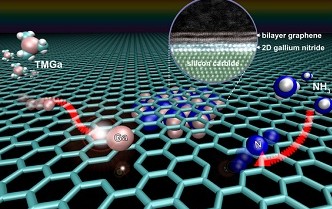
A newly discovered method for making two-dimensional materials could lead to new and extraordinary properties, particularly in a class of materials called nitrides, say the Penn State materials scientists who discovered the process. This first-ever growth of two-dimensional gallium nitride using graphene encapsulation could lead to applications in deep ultraviolet lasers, next-generation electronics and sensors.
"These experimental results open up new avenues of research in 2D materials," says Joshua Robinson, associate professor of materials science and engineering. "This work focuses on making 2D gallium nitride, which has never been done before."
Gallium nitride in its three-dimensional form is known to be a wide-bandgap semiconductor. Wide-bandgap semiconductors are important for high frequency, high power applications. When grown in its two-dimensional form, gallium nitride transforms from a wide-bandgap material to an ultrawide-bandgap material, effectively tripling the energy spectrum it can operate in, including the whole ultraviolet, visible and infrared spectrum. This work will have a particular impact on electro-optic devices that manipulate and transmit light.
"This is a new way of thinking about synthesizing 2D materials," said Zak Al Balushi, a Ph.D. candidate coadvised by Robinson and Joan Redwing, professor of materials science and engineering and electrical engineering. Al Balushi is lead author on a paper appearing online today (Aug.29) in the journal Nature Materials titled "Two-Dimensional Gallium Nitride Realized via Graphene Encapsulation."
"We have this palette of naturally occurring 2D materials," he continued. "But to expand beyond this, we have to synthesize materials that do not exist in nature. Typically, new material systems are highly unstable. But our growth method, called Migration Enhanced Encapsulated Growth (MEEG), uses a layer of graphene to assist the growth and stabilize a robust structure of 2D gallium nitride."
The graphene is grown on a substrate of silicon carbide, which is a technologically important substrate used widely in industry for LEDs, radar and telecommunications. When heated, the silicon on the surface decomposes and leaves a carbon-rich surface that can reconstruct into graphene. The advantage of producing the graphene in this way is that the interface where the two materials meet is perfectly smooth.
Robinson believes that in the case of two-dimensional gallium nitride, the addition of a layer of graphene makes all the difference. Graphene, a one-atom-thick layer of carbon atoms, is known for its remarkable electronic properties and strength.
"It's the key," Robinson says. "If you try to grow these materials the traditional way, on silicon carbide, you normally just form islands. It doesn't grow in nice layers on the silicon carbide."
When gallium atoms are added to the mix, they migrate through the graphene and form the middle layer of a sandwich, with graphene floating on top. When nitrogen atoms are added, a chemical reaction takes place that turns the gallium and nitrogen into gallium nitride.
"The MEEG process not only produces ultra-thin sheets of gallium nitride but also changes the crystal structure of the material, which may lead to entirely new applications in electronics and optoelectronics," said Redwing.
Additional coauthors include Ke Wang, Rafael Vila, Sarah Eichfield, Yu-Chuan Lin and Shruti Subramanian of Penn State, Ram Krishna Ghosh and Suman Datta of Notre Dame, Joshua Caldwell, U.S. Naval Research Laboratory, Xiaoye Qin and Robert Wallace The University of Texas at Dallas and Dennis Paul, Physical Electronics USA.
The Asahi Glass Co., Ltd, Japan, and the U.S. National Science Foundation provided funding for this project. The NSF Materials Science and Engineering Center at Penn State provided funding for Al Balushi. Other funding was provided by the Alfred P. Sloan Foundation, the Penn State Materials Characterization Laboratory and the Center for Low Energy Systems Technology (LEAST), funded by the Semiconductor Research Corporation and DARPA.
Share on:


Suggested Items
Groundbreaking Ceremony Marks the Beginning of a New Era for Newccess Industrial; The Construction of the MINGXIN Building
04/12/2024 | Newccess IndustrialOn a clear and sunny day in March, the groundbreaking ceremony for the MINGXIN Building took place in Shenzhen, China. This moment marked the official commencement of construction for a project that will reshape the semiconductor materials industry.
The Need for a Holistic Global Sustainability Standard
04/10/2024 | Michael Ford, Aegis SoftwareNo one can deny that the resources of our fragile planet are finite. The environment seems like a third party, subject to constant degradation. We’re acutely aware of the effects of pollution on our climate, and despite our “throw-away” culture, recycling and recovery of materials has remained relatively expensive, even as we use more energy just to survive.
iNEMI Publishes Four Roadmap Topics
04/04/2024 | iNEMIThe International Electronics Manufacturing Initiative (iNEMI) announces the availability of the first roadmap topics in the new iNEMI Roadmap format. Printed circuit boards, sustainable electronics, smart manufacturing, and mmWave materials and test are now available online.
Insulectro’s 'Storekeepers' Extend Their Welcome to Technology Village at IPC APEX EXPO
04/03/2024 | InsulectroInsulectro, the largest distributor of materials for use in the manufacture of PCBs and printed electronics, welcomes attendees to its TECHNOLOGY VILLAGE during this year’s IPC APEX EXPO at the Anaheim Convention Center, April 9-11, 2024.
Checking In With ICAPE Group
04/03/2024 | Nolan Johnson, I-Connect007ICAPE Group’s field application engineer Erik Pederson drills down on sustainability, supply chain resiliency, and what value engineering really looks like in this exclusive interview. Founded in 1999, European-based ICAPE Group provides 21 million printed circuit boards and over six million technical parts to manufacturers every month. With 30 PCB manufacturing partners globally and 50 partners providing a wide array of technical parts, ICAPE Group has operations in China, Taiwan, Thailand, South Korea, Vietnam, South Africa, Europe, Mexico, and the United States. The company also focuses on the value proposition for its customers.